PN Junction
In electronic engineering a PN junction describes a junction between a P-type and N-type semiconductor material. To understand what this means one need to know a little bit about semiconductors.

Some Semiconductor Basics
editIn a semiconductor material, such as silicon, the atoms have 4 electrons in the outermost electron energy band, called the valence band. This leaves room for 4 more electrons in the valence band, and these available "electron-slots", often referred to as holes, are easily borrowed by electrons from nearby atoms. Such materials will under the right conditions form a crystalline lattice where each atom borrows one electron from each of four nearby atoms.
By introducing atoms with different electron-configurations into the lattice we can create what referred to as a doped semiconductor. For example if we introduce the occasional boron atom to a silicon lattice we get a p-doped or p-type semiconductor. It is the fact that boron only has three valence electrons that makes it P-type, because this will leave occasional holes in the valence bands in the lattice. At room temperature these holes will move quite freely around in the material effectively making it a positive charge carrier, hence the name "p-type". Similarly a n-type semiconductor can be formed by doping the same silicon lattice with e.g. arsenic. Arsenic has 5 valence electrons and will at room temperature provide the material with easily movable electrons, which is a negative charge carrier, hence the name "n-type" semiconductor.
The PN-junction
editWhen a piece of semiconductor material changes type from p-type to n-type over a cross-section it forms a PN-junction. It is easy to think of it as two materials of different doping simply brought together, however in practice the junction is not formed that way. At temperatures well above absolute zero, holes from the p-side of the P-N junction will start to wander into the n-side due to thermal "vibrations". At the same time electrons from the n-side starts to wander into the p-side. This effect is called diffusion. The result is an excess of negative charge accumulating at the p-side and an excess of positive charge accumulating at the n-side. These changes in turn forms an electric field which counteracts the effect of the wandering charge-carriers (the electrons and holes) effectively stopping it at a distance into the opposite side. When the wandering electrons encounters the holes on the p-side they will fill the holes, and vice-versa. This leaves the area over the junction pretty much free of charge-carries. This area is called the depletion area, since it is depleted of charge-carriers. This is when the junction is not experiencing any outside electrical force.
The Bipolar Junction Diode
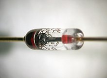
editThe simplest application of the PN junction is the bipolar junction diode (often made from silicon or germanium). A bipolar junction diode is basically a PN junction with conducting terminals attached to each side of the junction. The diode uses the properties caused by the depletion area of the junction. As the depletion area has very few free charge-carries it acts effectively as an insulator. If a voltage drop is applied from n- to the p-side of the diode the depletion area only gets wider, and very little current is allowed to pass through the diode. If we however apply a voltage drop form the p- to the n-side of the diode we will counteract the diffusion current and almost eliminate the depletion area, allowing a current to flow through the diode. The resulting effect is that the diode only carries current in one direction. As we need to overcome the electric field in the junction we will experience a voltage drop over the diode in the conducting direction. This is called the diode's threshold voltage, and is typically in the range 0.5-1V for standard off-the-shelf diodes. Even in the "non-conducting" direction diodes carry a small current due to a small amount of thermically generated charge-carriers in the depletion area. This is called the diode's leakage current.
Other Applications
editThe PN junction is essential to almost all modern electronics and is utilized in a lot of different components. It is the building block of the transistors that forms the basis for almost all digital electronics such as computers, and also most modern analog electronics such as audio amplifiers. It is essential in optical components such as light emitting diodes (LEDs) and semiconductor lasers, and an abundance of other more or less exotic electronic components.